CrossBar ReRAM: Rethinking Simplicity.
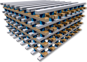
Resistive random-access memory (ReRAM) is based on a simple three-layer structure of a top electrode, switching medium and bottom electrode (FIGURE 1). The resistance switching mechanism is based on the formation of a filament in the switching material when a voltage is applied between the two electrodes. There are different approaches to implementing ReRAM, based on different switching materials and memory cell organization. Those variables drive significant performance differences depending upon the switching materials being used. In addition to use as multiple-time programmable (MTP), few-time programmable (FTP) and one-time programmable (OTP) non-volatile memory applications, CrossBar is offering its ReRAM technology for security applications, where ReRAM is used for secure physical unclonable function (PUF) keys embedded in semiconductors.

CrossBar ReRAM: Embedded – Scalable – Low Power – High Density
The approach is also CMOS compatible. Designers can put logic, controllers and microprocessors next to memory in the same die, simplifying packaging and increasing performance. ReRAM’s simple structure and CMOS compatibility enable any foundry - CMOS or logic - to enter the ReRAM business by licensing CrossBar ReRAM technology for Systems-on-Chip (SoC) or standalone memory devices or embedded cryptographic keys.
Read the “CrossBar ReRAM Technology” white paper to learn more: