ReRAM Overview

CrossBar ReRAM: Rethinking Simplicity.

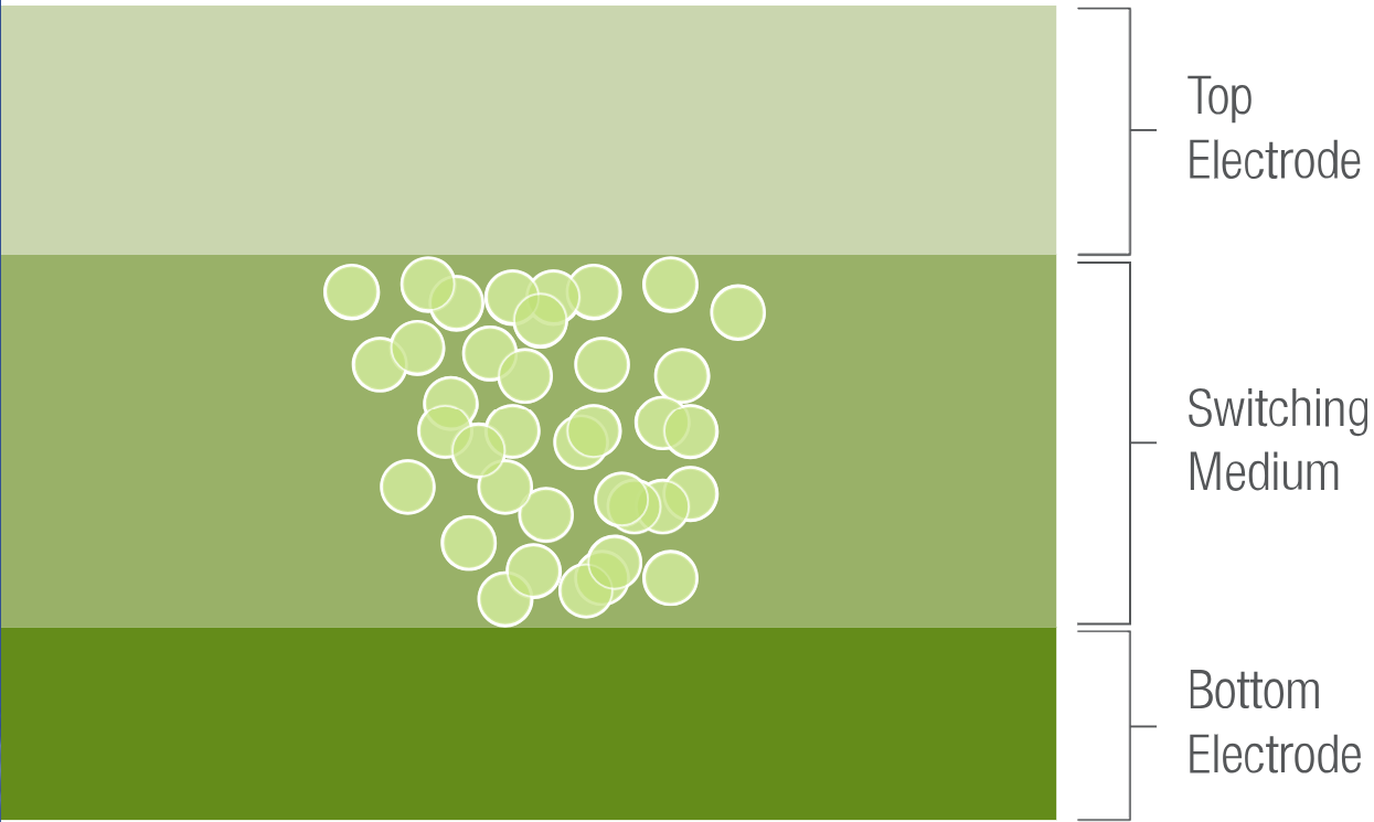
Resistive random-access memory (ReRAM) is based on a simple three-layer structure of a top electrode, switching medium and bottom electrode (Figure 1). The resistance switching mechanism is based on the formation of a filament in the switching material when a voltage is applied between the two electrodes. There are different approaches to implementing ReRAM, based on different switching materials and memory cell organization, making ReRAM highly adaptable for use as multiple-time programmable (MTP), few-time programmable (FTP) and one-time programmable (OTP) non-volatile memory applications.

Figure 1: ReRAM resistance switching mechanism (filament formation).
FIGURE 1. The resistance switching mechanism of CrossBar’s technology is based on the formation of a filament in the silicon-based switching material when a voltage is applied between the two electrodes.

ReRAM enables an all-in-one die solution giving users the utmost confidence in security from the chip level onwards. ReRAM is poised to be a key factor in the future of security with applications from traditional IoT to crypto wallet security.


CrossBar ReRAM: Embedded – Scalable – Low Power – High Density

Figure 2: Simple and scalable 3D ReRAM cell structure.
FIGURE 2. CrossBar’s simple and scalable memory cell structure enables a new class of 3D ReRAM which can be incorporated into the back end of line of any standard CMOS manufacturing fab.

CrossBar High-Density ReRAM technology can be stacked in 3D, delivering multiple terabytes of storage on a single chip. Its simplicity, stackability and CMOS compatibility enable logic and memory to be integrated onto a single chip at the latest technology node (Figure 2). CrossBar’s patented built-in selector allows various memory array configurations in which a single transistor can drive one or thousands of memory cells. This enables CrossBar cells to be organized in super dense 3D cross-point arrays, stackable with the capability to scale below 10nm, paving the way for terabytes on a single die.

Current Industry Problems

Limited Open Licensing

HW and SW from vendors often have partial or no OSS licenses.

Closed Chips and SEs

Even if OS is maximized, the chip HW is closed source.

Complex IP Stack

Chips necessarily integrate many types of 3rd-party IP.

Our Solution

MCU

  • Focus on flexibility, not security
  • Some logical security; generally no physical security
  • 40 nm and above, NVM is floating-gate flash in logic process
+

SE

  • Focus on security, not flexibility
  • Mature/commodity markets → perform decades-old functions at minimum cost
  • Does not support all blockchain signature types
  • Hard to go beyond “black box” usage

The approach is also CMOS compatible. Designers can put logic, controllers and microprocessors next to memory in the same die, simplifying packaging and increasing performance. ReRAM’s simple structure and CMOS compatibility enable any foundry — CMOS or logic — to enter the ReRAM business by licensing CrossBar ReRAM technology for Systems-on-Chip (SoC) or standalone memory devices or embedded cryptographic keys.

Read the “CrossBar ReRAM Technology” white paper to learn more:

OPEN PDF