
Overview of CrossBar Hardware: ReRAM and Chip
From ReRAM to SPU: The Hardware Foundation Powering Secure Self-Custody
The CrossBar Team
5/6/20269 min read
This article explores how Resistive Random Access Memory (ReRAM) became the foundation of CrossBar’s Secure Processing Unit (SPU) architecture. We explain how its security, durability, and scalability advantages over traditional flash memory enabled the design of CrossBar’s chip.


1. Resistive Random Access Memory (ReRAM): A Different Way to Store a Bit
In the first article of this series, our CEO Mark Davis introduced the company’s broader vision — how Resistive Random Access Memory (ReRAM) technology, the Secure Processing Unit (SPU) architecture, hardware products, applications, and open-source initiatives come together into a unified ecosystem. This article takes a closer look at the hardware behind that vision.
Built on more than 200 patents worldwide and years of custom chip design expertise, CrossBar’s platform is centered around ReRAM. That decision directly shaped Daric (the internal codename for CrossBar Chip 1), influencing its security architecture, advanced process node, and large on-chip memory capacity. To understand the chip, we first need to understand this memory technology behind it.
Every non-volatile memory (NVM) faces the same basic problem: keep the data when the power goes away. For decades, the dominant answer has been to trap a small amount of electrical charge on a node and call its presence (or absence) a “1” or a “0.” Flash, EEPROM, and SONOS all work this way. The cell holds its data for as long as the trapped charge stays put, which is typically rated in years.
Resistive Random Access Memory (ReRAM) takes a different approach. Instead of storing charge, a ReRAM cell stores a resistance. A thin dielectric film sits between two electrodes; applying a programming voltage causes conducting atoms to migrate and form (or dissolve) a tiny conducting filament. A high-resistance path means one state, a low-resistance path means the other. The data isn’t a charge that can leak — it’s a physical arrangement of atoms.
That sounds like a small distinction, but it changes almost everything downstream.
Simpler to Manufacture
The complexity of a chip process is largely driven by the number of photomasks it requires. Embedded flash typically adds 10 or more masks on top of a baseline logic process — about a 20–25% adder to the cost of a wafer. ReRAM adds only two masks, for roughly a 10% adder. Fewer steps mean fewer ways for things to go wrong, which generally means a more robust product.
This is also why ReRAM is practical at advanced nodes where flash isn’t. Embedded floating-gate flash is mostly stuck at 40nm and above; below that, the manufacturing trade-offs become brutal. ReRAM ports cleanly into smaller geometries, which is exactly why we can build Daric at 22nm — more on that below.
Better Retention Where People Actually Live
Retention specs are usually quoted at elevated temperatures (125°C or 150°C) because that’s where qualification tests run. The catch is that retention scales with the Arrhenius equation, and it scales with the activation energy of the failure mechanism. NOR flash has an activation energy of about 1.0 eV. ReRAM is around 1.5 eV.
Plug those numbers in: a flash and a ReRAM both rated for 10 years at 125°C will diverge sharply at the temperatures humans actually use them. At 100°C, the flash extrapolates to about 70 years of retention. The ReRAM extrapolates to 188 years. Higher activation energy means retention degrades faster as you heat the part up — but it also means retention improves much faster as you cool it down. That matters a lot for products that need to keep secrets reliably for the lifetime of the device and beyond.
Radiation Tolerance
Charge-based storage is, by definition, vulnerable to anything that creates mobile electron-hole pairs and dissipates the stored charge. Some flash devices begin to lose data at radiation levels around 25 krad, which is what you encounter in low-earth orbit. ReRAM, with no charge to lose, generally tolerates radiation in the hundreds of krad — enough for deep-space missions.
You don’t have to leave the atmosphere to care about this. X-ray inspection in board manufacturing, alpha particles from packaging materials, or just the slow accumulation of background radiation over a product’s life can all chip away at a flash bit. ReRAM is essentially indifferent to it.
For our products — where the bits in NVM are private keys and attestation roots — security is the headline benefit. Most published attacks on flash exploit the fact that the data is, fundamentally, charge:
Direct charge measurement. Backside sample preparation plus passive voltage contrast in an SEM can read flash contents. Not applicable to ReRAM — there’s no charge to measure.
Photon emission analysis. Switching transistors emit photons, and PEA can recover data from flash inside a microcontroller. ReRAM doesn’t switch charge in the same way, so PEA-based extraction doesn’t work on it.
Electron microscopy. Even high-resolution TEM can’t reliably resolve a ReRAM filament — it’s on the order of a single nanometer, smaller than the resolution at which you’d usefully tell the two states apart. And because the cell sits between metal layers in the back-end-of-line stack, plain SEM can’t see it at all.
Power analysis. ReRAM writes at around 3V vs. 10V+ for flash, doesn’t require a block-erase before writes, and reads at lower voltages and lower latency. Less power per operation means a smaller side-channel signal to differentiate.
Laser fault injection. Laser attacks against flash exploit the floating-gate transistor’s response to illumination. ReRAM doesn’t have that mechanism, so the same attacks don’t translate.
We didn’t want to take our own word for it, so we hired MicroNet Solutions to try to read out a ReRAM array using whatever they could throw at it: de-processing, electron imaging, focused-ion-beam milling, power analysis. They were unable to recover the contents.
A more complete treatment is in our ReRAM litepaper, but the headline is simple: when the data is “non-charge,” a whole category of attacks doesn’t apply.
Security: The Reason We Care Most
2. Daric: Building the World’s First SPU
ReRAM is a means to an end. The end is a chip that makes the right things easy and the wrong things hard for self-custody — and, more broadly, for any application where physical countermeasures and serious compute have to live together.
The existing market gives you two options:
An Microcontroller Unit (MCU) — flexible, fast, peripheral-rich, but with no real physical security.
A Secure Element (SE) — physically defended, but with a slow M0/M3-class core, tiny memory, and a fixed menu of decades-old crypto functions.
Wallet vendors have generally bolted these two chips together with a serial link in between. That works, sort of. But it leaves a couple of structural problems.
What’s Wrong With MCU + SE
Most off-the-shelf SEs don’t natively support the curves and primitives that modern blockchain and MPC protocols require — no secp256k1, no long RSA for Paillier keys, no hierarchical deterministic key derivation in-element. So in practice, the SE often gets demoted to “secure memory.” The private key gets reconstituted on the MCU side, and the actual signature math runs on a chip without physical countermeasures. The “EAL 6+” badge stays on the box, but the security boundary it implies has quietly moved.
Even when the SE does sign (Ledger is the notable exception, with a customized ST Micro firmware), the MCU still owns the user interface, key generation, and most of the application logic. A compromised MCU can present a fraudulent address on the display, capture user input, generate weak-entropy keys, or accept a flashed firmware image. Demonstrations of voltage glitching, light injection, and custom-firmware flashing on production wallets are well documented in the literature we cite in the Daric white paper.
Layered on top of all that: the I²C/SPI link between the two chips is itself an attack surface. Every signal that crosses it is observable, manipulable, and outside the security boundary of either die. Designing a protocol where each chip can reliably detect tampering of the other is famously hard.
And finally, both chips typically use floating-gate flash for their NVM — inheriting all the fragility and inspectability problems we just covered.
SPU
The Secure Processing Unit (SPU) is what you get when you stop accepting that trade-off. It’s an MCU and an SE, on a single die, in an advanced node, all under one umbrella of physical countermeasures, with ReRAM as the NVM.
Daric is our first instantiation. A few things worth highlighting on the architecture:
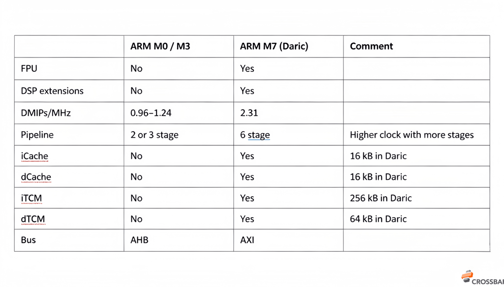
Two MCUs, not one. An ARM Cortex-M7 with MPU sits alongside a fully open source RISC-V (VexRiscv) with a true MMU. We were originally going to pick one, but the die-area cost of including both turned out to be a few cents — a remarkably good deal for the optionality it buys. The M7 is a real workhorse compared to the M0/M3 cores typical of SEs:
The RISC-V side runs at half the M7 clock but has something the M-series ARM cores don’t offer at all: a real MMU with memory virtualization. ARM keeps that feature for its A-series application processors. Having it on a security-focused MCU is an unusual operating point — Bunnie Huang’s write-up on Baochip-1x (the same tapeout as Daric) goes into why that matters.
A real crypto engine. The SE side has direct hardware acceleration for popular blockchain curves and signature types, hierarchical deterministic key generation in-element, RSA up to 6144 bits for Paillier keys, and multiple NIST 800–90B-compliant physical TRNGs with 800–90A post-processing. None of this requires copying private key material out to the MCU side.
ReRAM, on-chip, in quantity. Because we use ReRAM rather than flash, we can build at 22nm and afford to put unusually large code and data memory directly on-die. Big on-chip memory is itself a security feature — it keeps more of the system’s working state inside the PCM umbrella instead of on a board trace.
Why Integration Is the Real Win
A monolithic SPU isn’t just an MCU and an SE in a smaller package. The integration unlocks properties that are genuinely hard to get any other way:
Zero Trust by construction. Cryptographic operations, key management, UI handling, and blockchain-specific functions all live behind the same physical countermeasures. There’s no I²C/SPI link to snoop, no firmware-update protocol between chips to subvert, and no “trusted” bus to defend. We can write serial numbers, certificates, and attestation keys on the factory floor and have them validated at any point in the supply chain, including by the end user.
Atomic security policy enforcement. Lifecycle states, debug fuses, key-usage policies (no-export, sign-only), and attestation roots all sit on one die. There’s no inter-chip signaling to glitch in order to get a debug fuse to disagree with a lifecycle state. Tamper-detection circuits can monitor MCU, crypto engine, and ReRAM in real time and respond — wipe keys, lock the chip — without coordination.
Better side-channel posture. A multi-chip system makes it trivially easy to isolate the SE’s power signature in the lab. A monolithic SPU mixes cryptographic activity with everything else under unified power management, and the 22nm process gives us more options for noise shaping. The signal is still there in principle, but it’s a much messier signal.
Updateability that doesn’t open new holes. Firmware updates are signed and verified end-to-end inside one chip. No need to keep two firmware images, two lifecycle state machines, and an inter-chip update protocol all consistent and all secure.
The full argument, with citations to the relevant published attacks, is in the Daric white paper.
When viewed together, the relationship between ReRAM and the SPU architecture becomes clear. ReRAM provides a memory technology that is simpler to manufacture, more durable, more resistant to radiation, and significantly harder to attack than conventional flash. It also enables deployment at a 22nm process node, something that would be impractical with embedded flash technologies. That process advantage is what allows Daric to integrate both an ARM Cortex-M7 and a RISC-V processor, a dedicated cryptographic engine, and substantial on-chip memory within a practical die size, all protected under a unified PCM architecture. More importantly, that level of integration is what makes the security model fundamentally credible rather than merely conceptual.
Daric is more than a single chip — it is a proof of architecture. The next-generation successor currently in development, Denarius (the internal codename for CrossBar Chip 2), builds on the same foundation while extending the capabilities that have generated the strongest interest from developers and partners. We will share more details as development progresses.
In the meantime, the Daric SDK is live, the RTL of the open source Baochip-1x variant is available, and we’d love to hear what you build with it.
— The CrossBar Team